Graphene Patterned at Room Temp
Shadow mask etched for flexible substrates
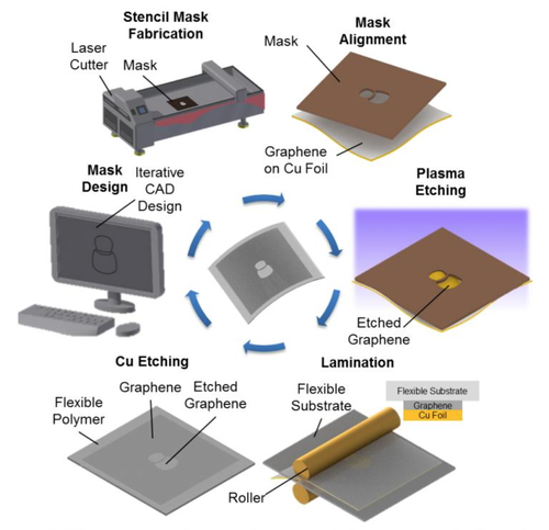
LAKE WALES Fla.—Graphene is easily grown with chemical vapor deposition (CVD) on copper foil, but a simple way of etching out the necessary circuit patterns and transferring them to a non-metallic substrate has eluded engineers. Now researchers at the University of Illinois (Urbana-Champaign) claim to have a one-step room temperature process for quickly patterning and transferring graphene circuits to flexible substrates using a simple shadow mask.
For years engineers have known that graphene can be easily deposited on copper foil using CVD, but nevertheless have wasted, according to these researchers, their time attempting to grow graphene on silicon substrates so their circuitry could be patterned using traditional techniques—from TI to IBM.
(Source: University of Illinois, Urbana-Champaign)
This room temperature method, instead takes the easily grown graphene-on-copper and in a single-step (they claim) etch and transfer the graphene circuitry to nearly any substrate, including the flexible polymer substrates of the future. Their trick: cutting the circuit patterns into a simple shadow mask.
"Desired micro-patterns are designed by a computer-aided design [CAD] software, enabling a commercial laser cutter interfaced to the computer to fabricate a shadow mask accordingly," doctoral candidate Keong Yong, from Professor SungWoo Nam's research group, told EE Times. "These rapid design iterations and pattern replications are facilitated by the quick turnover of the laser cutter to pattern low-cost polymer and metal sheets."
Once cut, the shadow mask is placed over the CVD-deposited graphene on copper foil, then etched using an oxygen plasma. The patterned graphene is then transferred onto a flexible substrate using a lamination process that ensures conformal contact and allows the copper foil to then be etched away.
"Due to this facile approach, our method reduces the total fabrication steps and time by eliminating the need for an intricate conventional micro-fabrication process as well as the need for a polymeric scaffold," Yong told EE Times. "More importantly, our polymer-free approach promotes cleaner graphene."
Right now there is no limitation on how big a graphene chip could be fabricated using their method, but there is a limit on how fine the shadow mask can be etched. To complete with silicon processing the shadow mask process has a ways to go, being confined to the micron range today, rather than nanometer range of silicon circuits today.
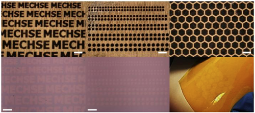
"We have demonstrated the capability of our facile approach to realize various graphene array patterns with different sizes, including lines, letters, and circles down to 50 microns," Yong told us.
Next the researchers aim to downsize their shadow masks and to build real devices to prove the concept that working graphene circuitry can indeed be fabricated in labs that cost thousands of dollars to equip rather than the billions required today, according to Yong.
Other contributors included post-doctoral researcher Pilgyu Kang and Ali Ashraf who has since graduated and now works at Intel.


