The knock against using graphene in digital electronics has been that it lacks an inherent band gap. However, over the years there have been a number of approaches that have been able to engineer a band gap into the material.
One of the most promising methods has been nitrogen doping, which actually increases the material’s conductivity rather than reduces it.
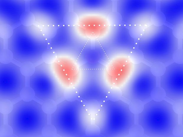
Now researchers at the U.S. Naval Research Laboratory (NRL) have developed a new technique for nitrogen doping of graphene that can control exactly where the dopants are placed in the graphene lattice. This precise localizing of the dopants reduces defects and provides greater material stability.
“Incorporation of nitrogen into the graphene lattice has been accomplished with other techniques including during the growth and post growth annealing processes,” explained Cory Cress, a researcher with NRL and a co-author of the papers, in an e-mail interview with IEEE Spectrum. “However, the technique we have employed is different in that we can control where the dopants are incorporated, both spatially and their depth (if using a multiply layer graphene sample). In general, the substitution of an impurity, like nitrogen, without additional defects is ideal for modifying the bandstructure since it best maintains the fundamental transport properties of graphene.”
Nitrogen’s particular qualities as a dopant for graphene are based on the fact that it has one more electron than carbon. When nitrogen is placed into the graphene lattice, all of its bonds are satisfied and the extra electron is free to move throughout the graphene layer. This increases the concentration of electrons in the material (also known as n-type doping) and increases the conductivity.
Previous studies have found that point defects generated in graphene (i.e., removal of one carbon atom) do not change the intrinsic doping level, according to Cress. “In other words, defects in graphene are charge-neutral so they can’t be used to controllably introduce a band-gap, although defects do degrade the transport due to increased defect scattering,” he said.
While other dopants fail on some level, nitrogen is the ideal n-type dopant for graphene when it is incorporated using the hyperthermal ion implantation (HyTII) process that the NRL researchers have employed. That’s because nitrogen has a similar mass and size as carbon, making the probability for substitution high.
The NRL researchers have described their HyTII process in the journal ACS Nano, and the characterization and measurements of the resulting material are described in the journal Physical Review B.
In their measurements, the NRL researchers observed a large negative magnetoresistance that scaled with the concentration of nitrogen implantation and a bandstructure alteration that can be precisely tunable with nitrogen content. Because it is in the lattice, the properties are fixed.
Adam L. Friedman, research physicist, NRL and first author of the paper, added in the press release: “Our measurements of these devices strongly indicate that we have finally fabricated a graphene film with a tunable bandgap, low defect density, and high stability. We therefore hypothesize that HyTII graphene films have great potential for electronic or spintronic applications for high-quality graphene where a transport or bandgap and high carrier concentration are desired.”


